How to Enhance the Luminous Efficiency of Germanium?

Although germanium has a direct band gap of 0.8 eV, it is essentially an indirect band gap material due to the presence of the L-conducting band.

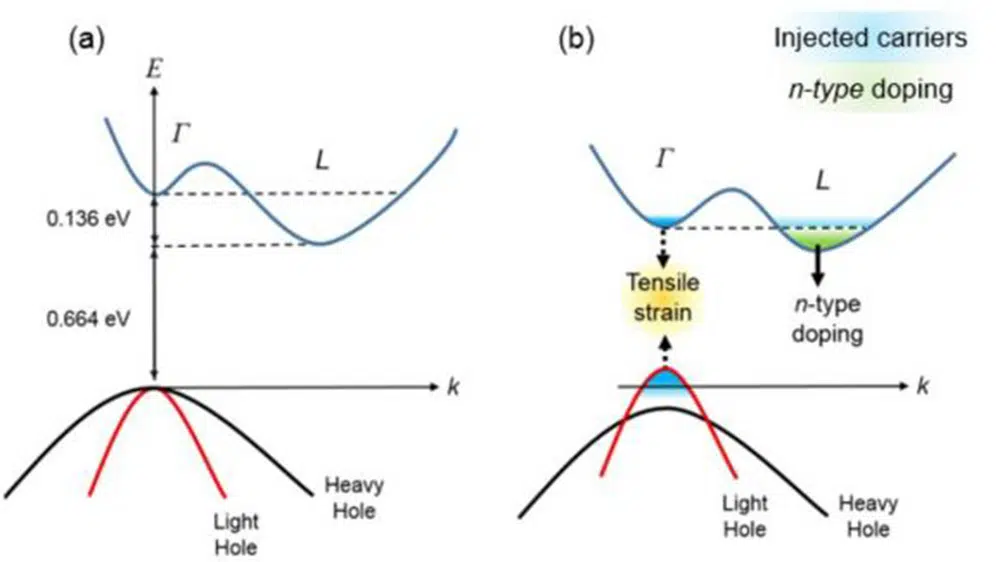
As shown in Fig. (a), this energy difference makes germanium an inefficient light emitter because most of the externally injected electrons will occupy the lower energy L conduction band valleys. When the compounding rate of the emitted photons is low, the electrons located in the L-conducting valleys can only be compounded with holes with the help of phonons, but by filling the indirect L-valleys in the conduction band, we can observe direct compounding at the r- point.

On the other hand, electrons located in the r-conducting valleys can be complexed with holes at a higher complexation rate. Thus, by making germanium a direct or pseudo-direct bandgap material, we increase the carrier complexation rate from the r-combination valley and make Ge an energy-efficient light emitter.

Direct optical gapping in germanium is a very fast process with a radiative compounding rate five orders of magnitude higher than indirect gapping. This means that direct gap emission in Ge is as efficient as in direct gap semiconductors. The luminescence of Ge can be significantly enhanced by utilizing the direct bandgap jump of Ge. 

Typically, Ge can be converted from an essentially indirect bandgap material to a direct bandgap material by introducing tensile strain, r-type doping, or Ge alloy with tin, as shown in figure (b) above. Both methods reduce the bandgap in the fault, i.e., the bandgap at the direct valleys is reduced at a higher rate than the indirect L-valleys, so that the bandgap structure of Ge is altered, ultimately transforming Ge into a direct bandgap material capable of absorbing or emitting light.

The above figure shows the germanium band gap diagram: (a) energy band engineering of bulk Ge and (b) Ge using tensile strain and n-type doping. Tensile strain reduces the energy difference between the T and L valleys, while n-type doping compensates for the remaining energy difference. The strain also induces a splitting of the light and heavy cavity bands, with greater luminosity expected as the tensile stress increases.

It has been shown theoretically that germanium can be engineered by tensile stress and n-type doping to achieve better direct bandgap photoemission at room temperature. Engineering the wrong bandgap by tensile stress opens up the possibility of developing novel optoelectronic devices that are fully compatible with silicon technology, such as light-emitting diode LEDs, lasers, and optical modulators. Ge has been used in a wide variety of devices ranging from energy-tunable light harvesters (e.g., photodetectors) to highly efficient optoelectronic devices.

Comments

Welcome to our blog dedicated to the attractive world of Germanium and other photoelectric materials. 
Get Our Quotation

Please let us know your request, we will get back to you within an hour.