Popular 4″ Germanium Substrate for LED Light Source

We have invested significant effort in expanding the application areas of current silicon-based complementary metal-oxide-semiconductor CMOS electronics to integrated photonics since 2003.

In particular, the monolithic integration of Group IV materials and their devices is mainly due to their compatibility with CMOS processes. Although key photonic devices such as modulators, waveguides, and detectors have been successfully integrated onto silicon-based electronic chips, the indirect bandgap nature of silicon limits the monolithic integration of high-efficiency light sources on its chips.

In contrast, germanium Ge, as a multi-valley indirect bandgap semiconductor material with both direct and indirect interband radiation complexes, possesses an energy band structure more suitable for direct bandgap inversion. 

It has been used to demonstrate high performance photodetectors, modulators, waveguides, and other optical components Recently, the interest in germanium as a Group I laser source has shown a significant growth after the use of optical and electrical injection to demonstrate optical gain and laser generation.

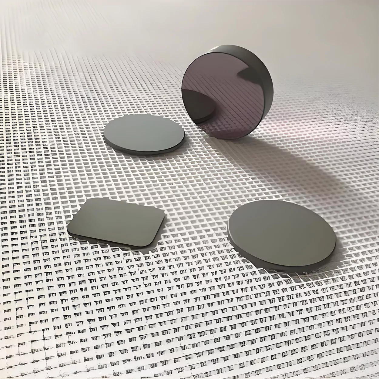
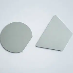
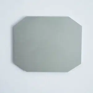
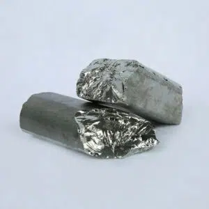
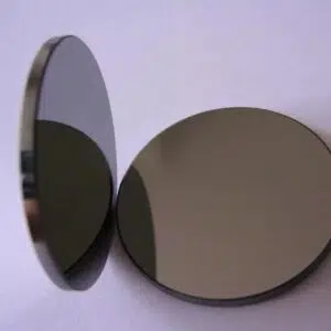
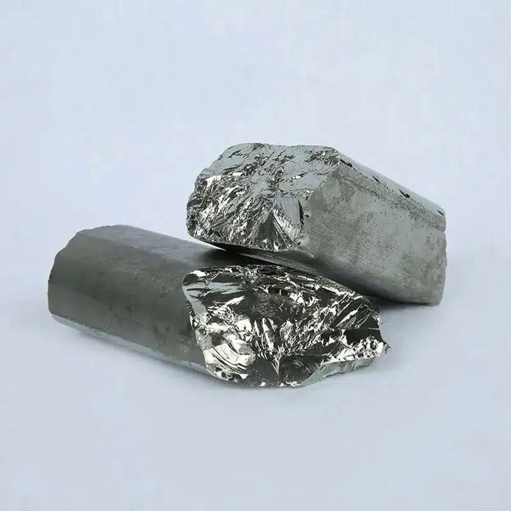
Available monocrystalline germanium substrates are used in the manufacture of LED light sources, with specific parameters detailed as follows.

ItemCN24 – Germanium Substrate
Diameter100mm(4″)
Thickness500μm,or as required
Crystal orientation<100>
DopingUndoped Intrinsically
Resistivity10-50 ohm-cm
GradeExcellent grade
Surface FinishDouble-sided polished, single-sided polished

Welcome to our blog dedicated to the attractive world of Germanium and other photoelectric materials. 
Get Our Quotation

Please let us know your request, we will get back to you within an hour.